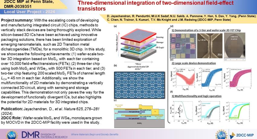
With the escalating costs of developing and manufacturing integrated circuit (IC) chips, methods to vertically stack devices are being thoroughly explored. While silicon-based 3D ICs have been achieved using innovative packaging solutions, there has been limited exploration of emerging nanomaterials, such as 2D Transition metal dichalcogenides (TMDs), for a monolithic 3D chip. In this study, we showcase the following achievements: (1) wafer-scale two-tier 3D integration based on MoS2, with each tier containing over 10,000 field-effect transistors (FETs); (2) three-tier chip using both MoS2 and WSe2, with 500 FETs in each tier; and (3) two-tier chip featuring 200 scaled MoS2 FETs of channel length LCH = 45 nm in each tier. Additionally, we show the multifunctionality of 2D materials by demonstrating a vertically connected 3D circuit, along with sensing and storage capabilities. This demonstration not only paves the way for the development of functionally divergent ICs, but also highlights the potential for 2D materials for 3D integrated chips.
2DCC Role: Wafer-scale MoS2 and WSe2 monolayers grown by MOCVD in the 2DCC-MIP facility were used in the study.
What Has Been Achieved: Bottom-up fabrication process for realizing monolithic 3D integrated (M3D) chips using large area MoS2 and WSe2. Demonstration of ultrascaled devices that are position directly above each other. Demonstration of multifunctionality on the upper tier of devices, as well as vertically integrated 3D inverter circuit.
Importance of the Achievement: This is the first demonstration of a three-tier 3D chip as well as wafer-scale 3D integration based on large-area-grown 2D materials. Unique Feature(s) of the MIP that Enabled this Achievement: 2DCC-MIP’s MOCVD growth of high-quality, wafer-scale MoS2 films.
Publication: D. Jayachandran, R. Pendurthi, M.U.K. Sadaf, N.U. Sakib, A. Pannone, C. Chen, Y. Han, N. Trainor, S. Kumari, T.V. Mc Knight, J.M. Redwing, Y. Yang, S. Das, “Three-dimensional integration of two-dimensional field-effect transistors,” Nature 2024, 625, 276-281. DOI: 10.1038/s41586-023-06860-5
Acknowledgements: We thank M. Labella and T. F. Schranghamer for developing the scaled lift-off process, and all staff of the Nanofabrication Lab at the Pennsylvania State University for their assistance. The MOCVD samples were grown in the 2D Crystal Consortium Materials Innovation Platform (2DCC-MIP) facility at the Pennsylvania State University, which is supported by the National Science Foundation under cooperative agreement DMR-2039351. This work was supported by the Army Research Office (ARO) through Contract Number W911NF1810268 and National Science Foundation (NSF) through CAREER Award under Grant Number ECCS-2042154. T.V.M. and J.M.R. acknowledge the support of the U.S. Air Force Office of Scientific Research and Clarkson Aerospace Corp. under Award no. FA9550-21-0460.
