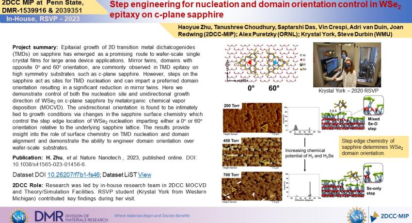
Epitaxial growth of 2D transition metal dichalcogenides (TMDs) on sapphire has emerged as a promising route to wafer-scale single crystal films for large area device applications. Mirror twins, domains with opposite 0° and 60° orientation, are commonly observed in TMD epitaxy on high symmetry substrates such as c-plane sapphire. However, steps on the sapphire act as sites for TMD nucleation and can impart a preferred domain orientation resulting in a significant reduction in mirror twins. Here we demonstrate control of both the nucleation site and unidirectional growth direction of WSe2 on c-plane sapphire by metalorganic chemical vapor deposition (MOCVD). The unidirectional orientation is found to be intimately tied to growth conditions via changes in the sapphire surface chemistry which control the step edge location of WSe2 nucleation imparting either a 0° or 60° orientation relative to the underlying sapphire lattice. The results provide insight into the role of surface chemistry on TMD nucleation and domain alignment and demonstrate the ability to engineer domain orientation over wafer-scale substrates.
2DCC Role: Research was led by in-house research team in 2DCC MOCVD and Theory/Simulation Facilities. RSVP student (Krystal York from Western Michigan) contributed key findings during her visit.
What Has Been Achieved: The study demonstrates the role that surface chemistry plays in controlling the nucleation of WSe2 domains at step edges on c-plane sapphire substrate. Under H2 and Se-rich growth conditions, the sapphire surface is fully passivated by Se atoms and the bottom edge of the step becomes the thermodynamically preferred site for nucleation, imparting a 60 degree orientation to the domains. However, when the growth ambient is less Se rich, the top edge of the step becomes the preferred site for nucleation resulting in a 0 degree domain orientation. In both cases, the percentage of mirror twin domains in the films after coalescence can be substantially reduced, to less than 15% areal coverage.
Importance of Achievement: Mirror twin domains in TMDs exhibit metallic behavior which can scatter carriers and reduce mobility. By reducing the number of mirror twins in monolayer films, the optical and electrical properties of the films are improved.
Unique Features of the MIP That Enabled Project: Close collaboration between in-house research teams in the Thin Films (MOCVD) Facility and the Theory/Simulation/Data Science Facility. RSVP program which enabled on-site participation by Krystal York.
Publication: Haoyue Zhu, Nadire Nayir, Tanushree H. Choudhury, Anushka Bansal, Benjamin Huet, Kunyan Zhang, Alexander A. Puretzky, Saiphaneendra Bachu, Krystal York, Thomas V. Mc Knight, Nicholas Trainor, Aaryan Oberoi, Ke Wang, Saptarshi Das, Robert A. Makin, Steven M. Durbin, Shengxi Huang, Nasim Alem, Vincent H. Crespi, Adri C.T. van Duin, Joan M. Redwing, “Step engineering for nucleation and domain orientation control in WSe2 epitaxy on c-plane sapphire,” Nature Nanotechnology, 2023, in press, https://doi.org/10.1038/s41565-023-01456-6.
Acknowledgments: The work was financially supported by the National Science Foundation (NSF) through the Pennsylvania State University 2D Crystal Consortium–Materials Innovation Platform (2DCC-MIP) under NSF cooperative agreement numbers DMR-1539916 and DMR-2039351. S.B. and N.A. acknowledge support provided by NSF Career grant number DMR-1654107. T.V.M. and J.M.R. acknowledge support from the Defense Technical Information Center under award number FA9550-21-1-0460. N.T. acknowledges support from the NSF Graduate Research Fellowship Program under grant number DGE1255832. K.Z. and S.H. acknowledge support from NSF under grant numbers ECCS-1943895 and ECCS-2246564 and Air Force Office of Scientific Research under grant number FA9550-22-1-0408. SHG measurements were supported by the Center for Nanophase Materials Sciences (CNMS), which is a US Department of Energy Office of Science User Facility at Oak Ridge National Laboratory.
