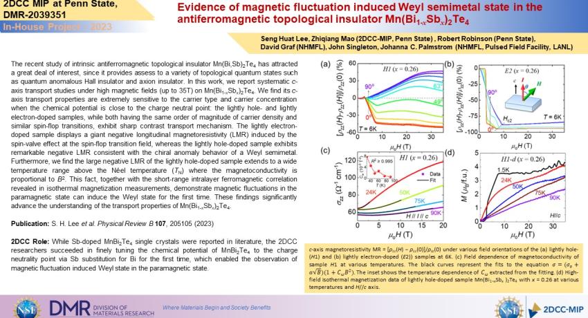
Emergent interfacial superconductivity at the interface of topology and magnetism

Heterogeneous interfaces that juxtapose different materials have been known to create emergent quantum phenomena. We used molecular beam epitaxy to synthesize heterostructures formed by stacking together two magnetic materials, a ferromagnetic topological insulator (Cr,Bi,Sb)2Te3 and an antiferromagnetic metal, iron chalcogenide (FeTe). High-resolution transmission electron microscopy (HRTEM) and x-ray diffraction show the formation of heterostructures with sharp interfaces and good crystallinity.