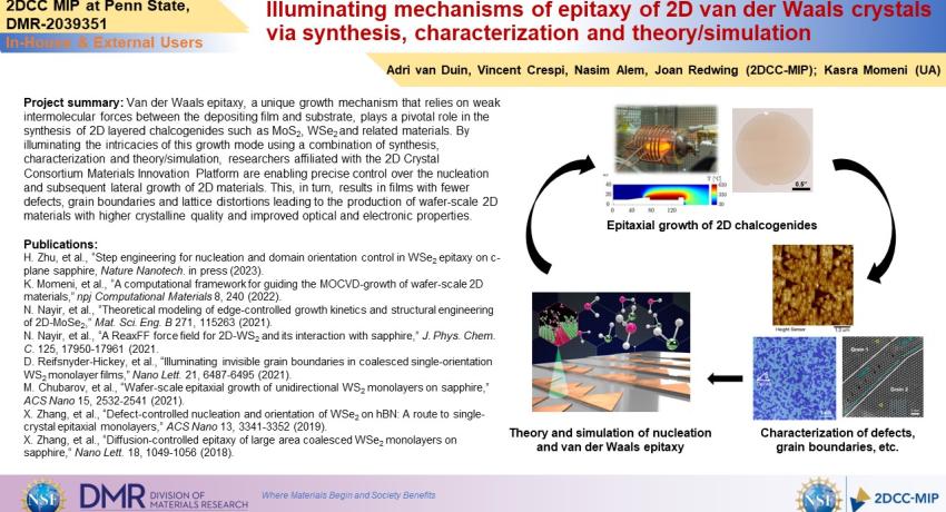
Van der Waals epitaxy, a unique growth mechanism that relies on weak intermolecular forces between the depositing film and substrate, plays a pivotal role in the synthesis of 2D layered chalcogenides such as MoS2, WSe2 and related materials. By illuminating the intricacies of this growth mode using a combination of synthesis, characterization and theory/simulation, researchers affiliated with the 2D Crystal Consortium Materials Innovation Platform are enabling precise control over the nucleation and subsequent lateral growth of 2D materials. This, in turn, results in films with fewer defects, grain boundaries and lattice distortions leading to the production of wafer-scale 2D materials with higher crystalline quality and improved optical and electronic properties.
Publications:
H. Zhu, et al., “Step engineering for nucleation and domain orientation control in WSe2 epitaxy on c-plane sapphire, Nature Nanotech. in press (2023).
K. Momeni, et al., “A computational framework for guiding the MOCVD-growth of wafer-scale 2D materials,” npj Computational Materials 8, 240 (2022).
N. Nayir, et al., “Theoretical modeling of edge-controlled growth kinetics and structural engineering of 2D-MoSe2,” Mat. Sci. Eng. B 271, 115263 (2021).
N. Nayir, et al., “A ReaxFF force field for 2D-WS2 and its interaction with sapphire,” J. Phys. Chem. C. 125, 17950-17961 (2021).
D. Reifsnyder-Hickey, et al., “Illuminating invisible grain boundaries in coalesced single-orientation WS2 monolayer films,” Nano Lett. 21, 6487-6495 (2021).
M. Chubarov, et al., “Wafer-scale epitaxial growth of unidirectional WS2 monolayers on sapphire,” ACS Nano 15, 2532-2541 (2021).
X. Zhang, et al., “Defect-controlled nucleation and orientation of WSe2 on hBN: A route to single-crystal epitaxial monolayers,” ACS Nano 13, 3341-3352 (2019).
X. Zhang, et al., “Diffusion-controlled epitaxy of large area coalesced WSe2 monolayers on sapphire,” Nano Lett. 18, 1049-1056 (2018).
What Has Been Achieved: The research is aimed at understanding fundamental mechanisms of van der Waals epitaxy of transition metal dichalcogenide monolayers and related 2D chalcogenides to achieve wafer-scale films with reduced defects and grain boundaries to provide electronic grade material to advance device applications. Detailed experimental studies of nucleation, domain growth and coalescence are combined with DFT and ReaxFF force field-based molecular dynamic simulations to provide key insights. The work has led to development of wafer-scale processes for epitaxial growth of WS2 and WSe2 monolayers with significantly reduced inversion domains, identification of growth modes responsible for translational line defects in the films and insights into the role of dislocations in TMD epitaxy on twisted and non-twisted bilayer graphene.
Importance of the Achievement: The availability of wafer-scale single crystal TMD monolayer and few-layer films is needed to advance large scale device applications. 2DCC-MIP is one of the leading groups worldwide developing reproducible processes for high crystalline quality 2D chalcogenide films.
Unique Feature(s) of the MIP that Enabled this Achievement: The effort involves a close collaboration between in-house researchers in the 2DCC-MIP Thin Films and In-Situ Characterization Facility and the Theory/Simulation/Data Science Facility as well as external user groups. The research is enabled by 2DCC tools equipped for uniform synthesis of TMD films on 2” diameter substrates and expertise in DFT/ReaxFF simulations.
