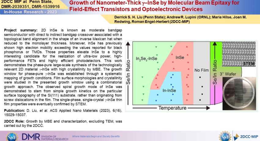
2D InSe is known as a moderate bandgap semiconductor with direct to indirect bandgap crossover associated with a topological band alignment in the shape of an inverse Mexican hat when reduced to the monolayer thickness. Moreover, InSe has previously shown high electron mobility exceeding the values reported for black phosphorus or TMDs. Those properties elevate InSe to a highly interesting candidate for the realization of ultra-low power, high-performance FETs and highly efficient photodetectors. This work demonstrates the phase-pure large-scale synthesis of the technologically relevant 2D material g-InSe with high crystallinity by MBE. The growth window for phase-pure g-InSe was established through a systematic mapping of growth conditions. Film surface morphologies and crystallinity were studied in the presented growth window using a combinatorial growth approach. The observed spiral growth mode of InSe was demonstrated to stem from simple growth kinetics on the particular surface topography of the Si(111) substrate, rather than originating from screw dislocations in the film. The single-phase, single-crystal g-InSe thin film properties were eventually confirmed by STEM.
2DCC Role: Growth by MBE and characterization, excluding TEM, was carried out by the 2DCC.
What Has Been Achieved: We have demonstrated single-phase, single-crystal thin film growth of g-InSe over 3 inches Si(111) wafer size by MBE. Using a combinatorial growth approach for the first time for 2D material growth, the phase diagram and growth window for g-InSe was mapped out systematically and crystal properties and film surface morphology of the obtained g-InSe films were studied.
Importance of Achievement: 2D material growth over large areas remains challenging for thin film bottom-up growth approaches. However, a scalable fabrication process for high-mobility 2D semiconductors is technologically highly relevant. This work successfully demonstrated the large-area growth of g-InSe with excellent crystal properties and in single phase.
Unique Features of the MIP That Enabled Project: Capability to grow InSe with MBE on 3 inches wafer size.
Publication: Derrick S. H. Liu, Maria Hilse, Andrew R. Lupini, Joan M. Redwing, and Roman Engel-Herbert, “Growth of Nanometer-Thick g-InSe on Si(111) by Molecular Beam Epitaxy for Field-Effect Transistors and Optoelectronic Devices,” ACS Applied Nano Materials 6 (16), 15029-15037 (2023). https://doi.org/10.1021/acsanm.3c12345.
Acknowledgments: U.S. Department of Energy, Office of Science, Office of Basic Energy Sciences Energy Frontier Research Center programs under Award no. DE-SC0021118. NSF cooperative Agreements Number DMR-1539916 and DMR-2039351. U.S. Department of Energy, Office of Basic Energy Sciences, Division of Materials Sciences and Engineering, and Center for Nanophase Materials Sciences, a U.S. Department of Energy, Office of Science User Facility at Oak Ridge National Laboratory under Contract no. DE-AC05-00OR22725.
