

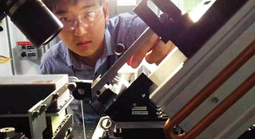
Xiaoyu Ji, Ph.D. candidate in materials science at Penn State, tests his crystals at Argonne National Laboratory with beamline scientist Wenjun Liu. The work was done at the sector and beamline no. 34-ID-E at the Advanced Photon Source.
A new method to improve semiconductor fiber optics may lead to a material structure that might one day revolutionize the global transmission of data, according to an interdisciplinary team of researchers.
Researchers are working with semiconductor optical fibers, which hold significant advantages over silica-based fiber optics, the current technology used for transmitting nearly all digital data. Silica — glass — fibers can only transmit electronic data converted to light data. This requires external electronic devices that are expensive and consume enormous amounts of electricity. Semiconductor fibers, however, can transmit both light and electronic data and might also be able to complete the conversion from electrical to optical data on the fly during transmission, improving delivery speed.
Think of these conversions as exit ramps on the information superhighway, said Venkatraman Gopalan, professor of materials science and engineering, Penn State. The fewer the exits the data takes, the faster the information travels. Call it "fly-by optoelectronics," he said.
In 2006, researchers, led by John Badding, professor of chemistry, physics, and materials science and engineering, first developed silicon fibers by embedding silicon and other semiconductor materials into silica-fiber capillaries. The fibers, comprised of a series of crystals, were limited in their ability to transmit data because imperfections, such as grain boundaries at the surfaces where the many crystals within the fiber core bonded together, forced portions of the light to scatter, disrupting the transmission.
A method designed by Xiaoyu Ji, doctoral candidate in materials science and engineering, improves on the polycrystalline core of the fiber by melting a high-purity amorphous silicon core deposited inside a 1.7-micron inner-diameter glass capillary using a scanning laser, allowing for formation of silicon single crystals that were more than 2,000 times as long as they were thick. This method transforms the core from a polycrystal with many imperfections to a single crystal with few imperfections that transmits light much more efficiently.
Read the full news story here:
http://news.psu.edu/story/461805/2017/04/11/research/method-improves-semicond...