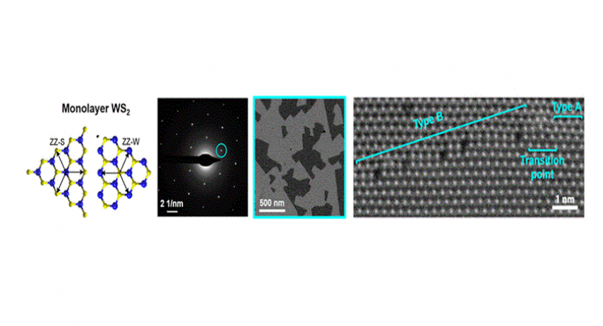
Three images of tungsten disulfide (WS2) monolayer on the left show results from several complementary transmission electron microscopy techniques that show evidence of nearly single-crystalline films with translational grain boundary defect arrays. The crystal structure model of a WS2 monolayer on the right shows how two similarly oriented crystal edges approach each other during growth, inducing out-of-plane tilts at the grain boundaries. Image: Penn State Materials Research Institute
By Jamie Oberdick
Two-dimensional materials are essential for developing new ultra-compact electronic devices, but producing defect-free 2D materials is a challenge. However, discovery of new types of defects in these 2D materials may give insight into how to create materials without such imperfections, according to a group of Penn State researchers.
“2D materials are exciting new materials for electronics, and because they are so thin, they make it possible to shrink devices to very small sizes,” said Danielle Reifsnyder Hickey, Penn State assistant research professor of materials science and engineering. “This is critical for making electronics more powerful so that they can handle more data. However, it is a huge challenge to grow perfect 2D materials over areas large enough to be able to make large arrays of high-quality devices.”
Reifsnyder Hickey and the team of Penn State researchers have discovered new types of defects that provide clues for a way to create defect-free 2D materials. The study recently appeared in Nano Letters.
"We found new defects that are on the Angstrom scale, at one-tenth of a nanometer, and we were able to correlate the atomic structure to very large scales, at several microns,” said Nasim Alem, Penn State associate professor of materials science and engineering and the study’s corresponding author.
The team studied defects in monolayer films of tungsten disulfide grown by the research group of Joan Redwing, professor of materials science and engineering, Penn State. Tungsten disulfide belongs to a class of 2D crystals known as transition metal dichalcogenides, which are three-atom-thick crystals that have properties that make them ideal for the development of future electronics.
“2D material monolayers have different properties than bulk crystals,” Reifsnyder Hickey said. “For example, they have direct band gaps and can therefore be used as very small transistor materials, and their crystal symmetry enables new types of devices based on increased degrees of freedom relative to their bulk counterparts.”
A direct band gap is an ideal feature for exciting an electron into a conducting energy state to allow the flow of electricity. Semiconductor technology, for example, is reliant on the manipulation of electronic charge in this way. Recently, spin and valley degrees of freedom have also shown promise in 2D materials and can be manipulated to enable new types of devices. For instance, orienting multiple spins in a material can lead to magnetism, and distributing electrons among different local minimum and maximum energy states — valleys — that possess the same energy but occur with different momentum values can enable new ways to process and store information. A key to unlocking the potential of these properties is growing defect-free films, which can be achieved only by identifying and understanding atomic defects, as was achieved in this work.
The defects the team discovered are known as translational grain boundaries, which occur at the interface between two crystallites that have the same orientation but a translational offset. Typically, grain boundaries connect grains with dissimilar orientations and can affect the material's properties such as thermal and electrical conductivity, lessening their value for electronics. To investigate the unusual translational grain boundaries, the team used a combination of scanning transmission electron microscopy imaging and a ReaxFF reactive force field simulation. ReaxFF was developed by Adri van Duin, a Penn State distinguished professor of mechanical engineering who also participated in the study.
The research found that the translational grain boundaries identified exist as subtle but widespread imperfections in the monolayer films.
“Through a synergistic approach, we were able to explain our experimental findings using simulations and uncover the growth mechanism that leads to such microstructure,” Alem said. “This is an important step, because by learning the underlying physics of growth and defect formation, we can learn to modify and control them, and this will have a profound effect of the electronic properties of the crystal.”
Improving the material would lead to better electronics, according to Reifsnyder Hickey.
“This investigation experimentally discovered the structures and used theory and simulation to correlate their formation with the growth conditions,” Reifsnyder Hickey said. “Now, we would like to implement what we have learned, so that these offsets in grains can be eliminated to form truly single-crystalline films large enough for excellent electronics. We would also like to explore the properties of these and related atomic defects.”
Being able to produce improved electronics based on tungsten disulfide monolayer films with minimal defects is good news for an increasingly visual society, according to Reifsnyder Hickey.
“A couple decades ago, it was unheard of to watch a video on a telephone,” Reifsnyder Hickey said. “But now, we consume a lot of information visually, especially with videos, including news, communication and entertainment. Because electronics have become so powerful, we are able to easily carry in our pockets the devices that enable this. Our findings could lead to a new generation of such devices.”
Other Penn State researchers involved in the study include Nadire Nayir, Mikhail Chubarov, Tanushree H. Choudhury, Saiphaneendra Bachu, Leixin Miao, Yuanxi Wang, Chenhao Qian and Vincent H. Crespi.
The National Science Foundation through the Penn State 2D Crystal Consortium-Materials Innovation Platform and an NSF CAREER award to Nasim Alem supported this research.
Read the full news story here:
https://news.psu.edu/story/664966/2021/08/02/research/finding-new-types-2d-ma...

