
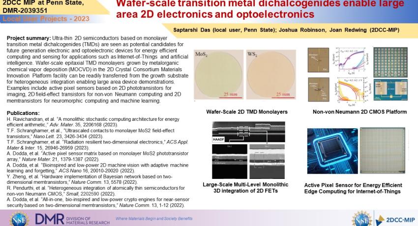
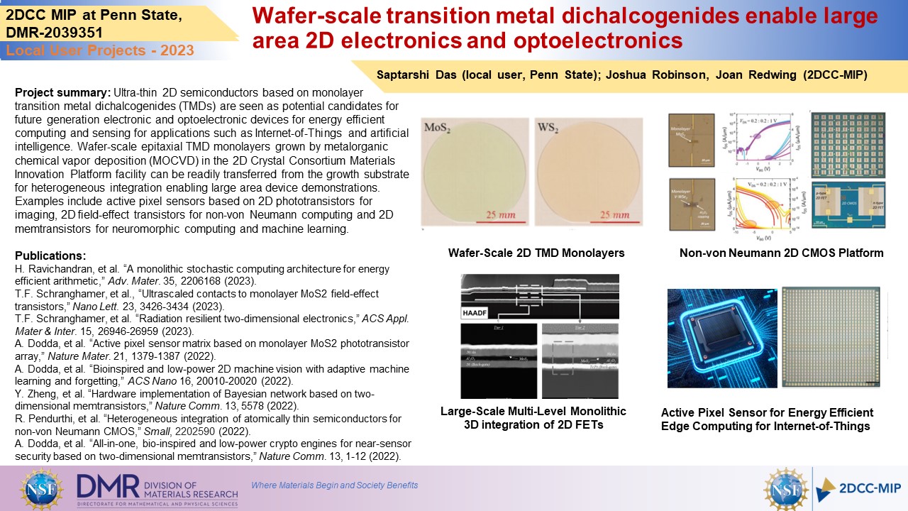
Ultra-thin 2D semiconductors based on monolayer transition metal dichalcogenides (TMDs) are seen as potential candidates for future generation electronic and optoelectronic devices for energy efficient computing and sensing for applications such as Internet-of-Things and artificial intelligence. Wafer-scale epitaxial TMD monolayers grown by metalorganic chemical vapor deposition (MOCVD) in the 2D Crystal Consortium Materials Innovation Platform facility can be readily transferred from the growth substrate for heterogeneous integration enabling large area device demonstrations. Examples include active pixel sensors based on 2D phototransistors for imaging, 2D field-effect transistors for non-von Neumann computing and 2D memtransistors for neuromorphic computing and machine learning.
Publications:
H. Ravichandran, et al. “A monolithic stochastic computing architecture for energy efficient arithmetic,” Adv. Mater. 35, 2206168 (2023).
T.F. Schranghamer, et al., “Ultrascaled contacts to monolayer MoS2 field-effect transistors,” Nano Lett. 23, 3426-3434 (2023).
T.F. Schranghamer, et al. “Radiation resilient two-dimensional electronics,” ACS Appl. Mater & Inter. 15, 26946-26959 (2023). A. Dodda, et al. “Active pixel sensor matrix based on monolayer MoS2 phototransistor array,” Nature Mater. 21, 1379-1387 (2022).
A. Dodda, et al. “Bioinspired and low-power 2D machine vision with adaptive machine learning and forgetting,” ACS Nano 16, 20010-20020 (2022).
Y. Zheng, et al. “Hardware implementation of Bayesian network based on two-dimensional memtransistors,” Nature Comm. 13, 5578 (2022).
R. Pendurthi, et al. “Heterogeneous integration of atomically thin semiconductors for non-von Neumann CMOS,” Small, 2202590 (2022).
A. Dodda, et al. “All-in-one, bio-inspired and low-power crypto engines for near-sensor security based on two-dimensional memtransistors,” Nature Comm. 13, 1-12 (2022).
What Has Been Achieved: Wafer-scale transition metal dichalcogenide monolayer and few-layer films developed in the 2DCC-MIP facility have enabled large area device demonstrations.
Importance of the Achievement: TMD monolayers grown by metalorganic chemical vapor deposition (MOCVD) in the 2DCC-MIP facility can be readily transferred from the growth substrate for heterogeneous integration enabling large area device demonstrations. Examples include active pixel sensors based on 2D phototransistors for imaging, 2D field-effect transistors for non-von Neumann computing and 2D memtransistors for neuromorphic computing and machine learning.
Unique Feature(s) of the MIP that Enabled this Achievement: The development of reproducible, uniform TMD films with high crystalline quality on wafer-scale substrates.