
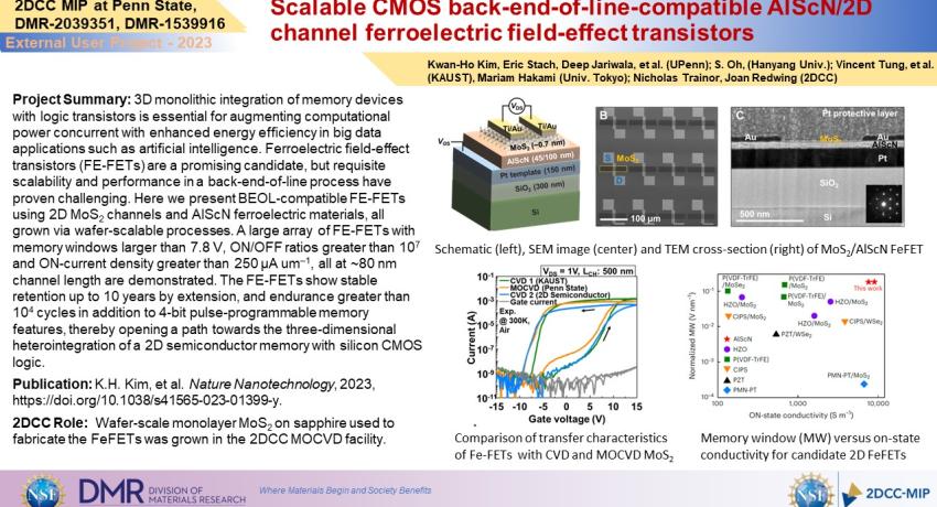
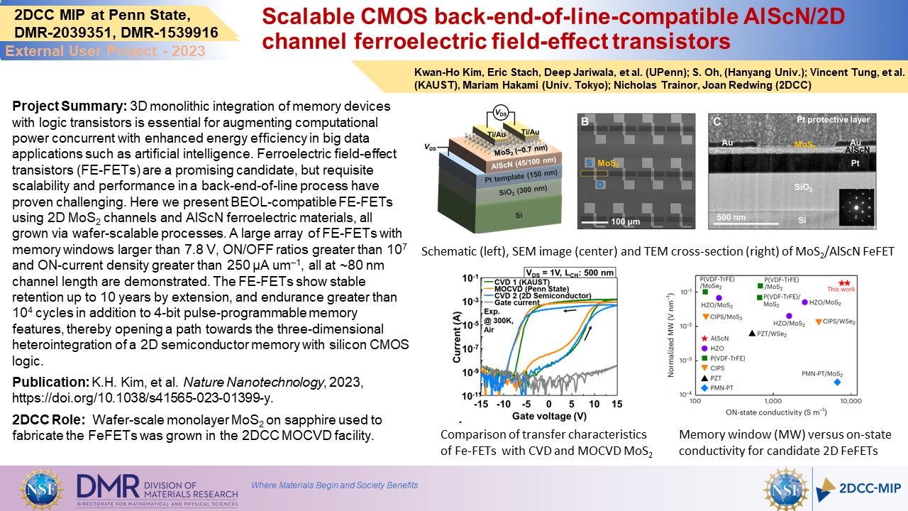
3D monolithic integration of memory devices with logic transistors is essential for augmenting computational power concurrent with enhanced energy efficiency in big data applications such as artificial intelligence. Ferroelectric field-effect transistors (FE-FETs) are a promising candidate, but requisite scalability and performance in a back-end-of-line process have proven challenging. Here we present BEOL-compatible FE-FETs using 2D MoS2 channels and AlScN ferroelectric materials, all grown via wafer-scalable processes. A large array of FE-FETs with memory windows larger than 7.8 V, ON/OFF ratios greater than 107, and ON-current density greater than 250 μA μm−1, all at ~80 nm channel length, are demonstrated. The FE-FETs show stable retention up to 10 years by extension, and endurance greater than 104 cycles in addition to 4-bit pulse-programmable memory features, thereby opening a path towards the three-dimensional heterointegration of a 2D semiconductor memory with silicon CMOS logic.
Publication: K.H. Kim, et al. Nature Nanotechnology, 2023, https://doi.org/10.1038/s41565-023-01399-y.
2DCC Role: Wafer-scale monolayer MoS2 on sapphire used to fabricate the FeFETs was grown in the 2DCC MOCVD facility.
What Has Been Achieved: This study has demonstrated FeFETs fabricated using a 2D MoS2 channel and AlScN ferroelectric layer fabricated using scalable BEOL-compatible processing (<450°C). The devices exhibit large memory windows and stable retention and endurance.
Importance of the Achievement: The concept of FE-FET memory has been pursued since the 1960s, since these devices could operate at extremely low powers. However, it has been challenging to fabricate devices at temperatures (<450°C) that are compatible with silicon CMOS logic. The 2D channel materials are also so thin that once a memory bit is written in them, they preserve that information in the form of charge for years.
Unique Feature(s) of the MIP that Enabled this Achievement: 2DCC-MIP’s MOCVD growth of high-quality, wafer-scale MoS2 films. The growth of high-quality monolayer MoS2 films enabled us to fabricate large area arrays of FE-FETs.
Publication: K.W. Kim, S. Oh, M.M.A. Fiagbenu, J. Zheng, P. Musavigharavi, P. Kumar, N. Trainor, A. Aljarb, Y. Wan, H.M. Kim, K. Katti, S. Song, G.W. Kim, Z. Tang, J.H. Fu, M. Hakami, V. Tung, J.M. Redwing, E.A. Stach, R.H. Olsson III, D. Jariwala, "Scalable CMOS back-end-of-line-compatible AlScN/two-dimensional channel ferroelectric field-effect transistors," Nature Nanotechnology, published online May 2023. https://doi.org/10.1038/s41565-023-01399-y.
Acknowledgements: This material is based on work supported by the Defense Advanced Research Projects Agency (DARPA) TUFEN program under agreement no. HR00112090046. The work was carried out in part at the Singh Center for Nanotechnology at the University of Pennsylvania, which is supported by the National Science Foundation (NSF) National Nanotechnology Coordinated Infrastructure Program (NSF grant NNCI-1542153). H.M.K., K.K., and D.J. acknowledge partial support from the Penn Center for Undergraduate Research and Fellowships. We gratefully acknowledge the use of the facilities and instrumentation supported by NSF through the University of Pennsylvania Materials Research Science and Engineering Center (MRSEC) (DMR-1720530). P.K., E.A.S., and D.J. also acknowledge partial support from the NSF DMR Electronic Photonic and Magnetic Materials (EPM) core program (grant no. DMR-1905853) as well as the University of Pennsylvania Laboratory for Research on the Structure of Matter, a Materials Research Science and Engineering Center (MRSEC) supported by the NSF (no. DMR-1720530).
A.A., Y.W., and V.C.T. are indebted to the support from the King Abdullah University of Science and Technology (KAUST) Solar Center and Office of Sponsored Research (OSR) under award no. OSR-2018-CARF/CCF-3079. The MOCVD-grown MoS2 monolayer samples were provided by the 2D Crystal Consortium—Materials Innovation Platform (2DCC-MIP) facility at the Pennsylvania State University, which is funded by the NSF under cooperative agreement nos. DMR-1539916 and DMR-2039351. S.S. acknowledges support from the Basic Science Research Program through the National Research Foundation of Korea (NRF) funded by the Ministry of Education (grant no. 2021R1A6A3A14038492). K.K. acknowledges support from the NSF Graduate Research Fellowship Program (GRFP), Fellow ID: 2022338725. N.T. acknowledges that this material is based upon work supported by the National Science Foundation Graduate Research Fellowship Program under Grant No. DGE1255832.