
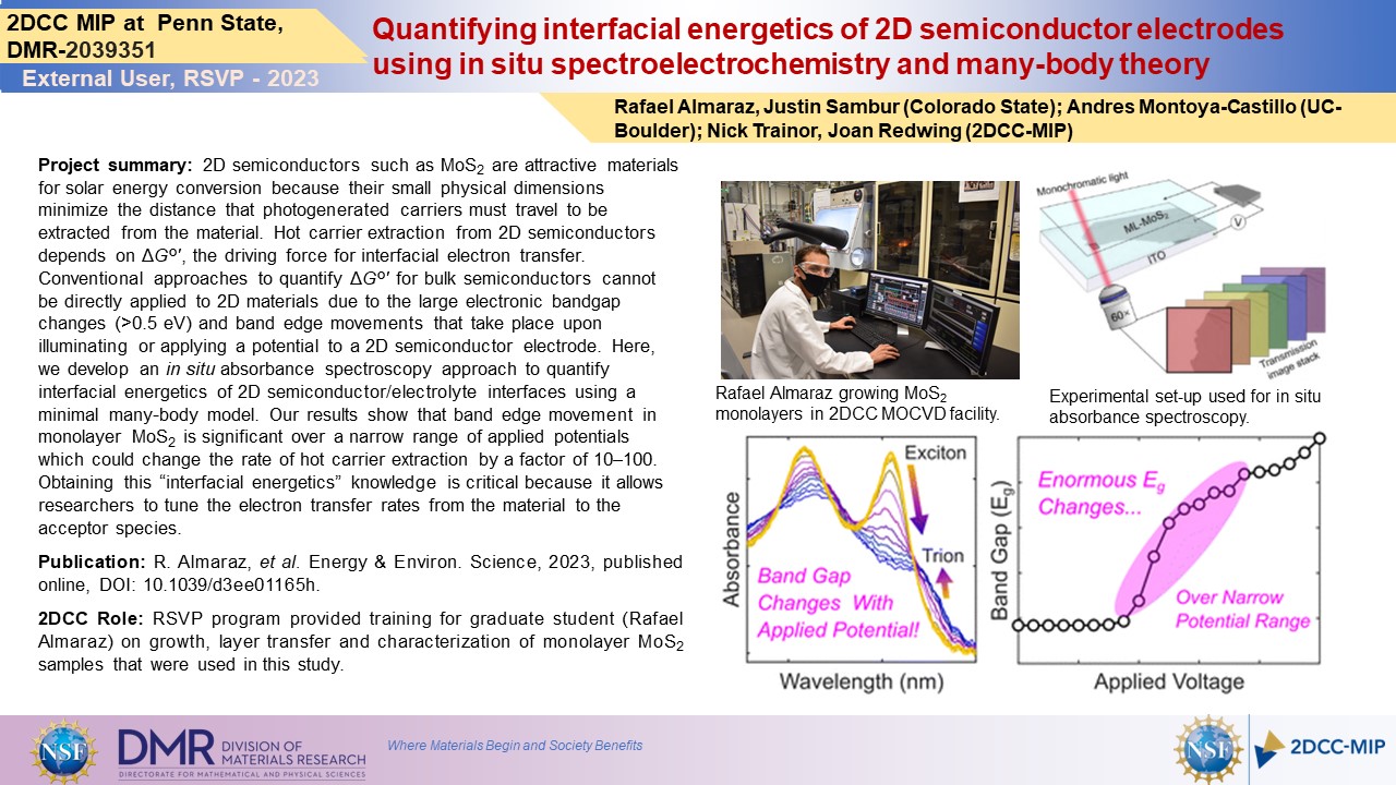
2D semiconductors such as MoS2 are attractive materials for solar energy conversion because their small physical dimensions minimize the distance that photogenerated carriers must travel to be extracted from the material. Hot carrier extraction from 2D semiconductors depends on ΔG°′, the driving force for interfacial electron transfer. Conventional approaches to quantify ΔG°′ for bulk semiconductors cannot be directly applied to 2D materials due to the large electronic bandgap changes (>0.5 eV) and band edge movements that take place upon illuminating or applying a potential to a 2D semiconductor electrode. Here, we develop an in situ absorbance spectroscopy approach to quantify interfacial energetics of 2D semiconductor/electrolyte interfaces using a minimal many-body model. Our results show that band edge movement in monolayer MoS2 is significant over a narrow range of applied potentials which could change the rate of hot carrier extraction by a factor of 10–100. Obtaining this “interfacial energetics” knowledge is critical because it allows researchers to tune the electron transfer rates from the material to the acceptor species.
2DCC Role: RSVP program provided training for graduate student (Rafael Almaraz) on growth, layer transfer and characterization of monolayer MoS2 samples that were used in this study.
What Has Been Achieved: The energetics of interfacial electron transfer of a 2D semiconductor/electrolyte interface were studied using in situ absorbance spectroscopy. The results demonstrate significant changes in the band gap and conduction band/valence band edge in MoS2 with changes in the applied potential which could change the rate of hot carrier extraction by a factor of 10-100.
Importance of Achievement: 2D semiconductors such as MoS2 are attractive materials for solar energy conversion due to their strong absorption and small physical dimensions which facilitates extraction of photogenerated carriers from the material. However, conventional approaches that are used to understand the interfacial energetics of bulk semiconductor/electrolyte interfaces cannot be directly applied. This study provides insights into the effects of the applied electrode potential on the band gap and band edge position of MoS2 which are needed to understand the interfacial energetics of the system.
Unique Features of the MIP That Enabled Project: RSVP training program which provided housing and travel support for Rafael Almaraz to work in the 2DCC facility to become proficient with MOCVD growth, layer transfer and characterization of monolayer MoS2 films.
Publication: Rafael Almaraz, Thomas Sayer, Justin Toole, Rachelle Austin, Yusef Farah, Nicholas Trainor, Joan M. Redwing, Amber Krummel, Andres Montoya-Castillo, Justin Sambur, Energy & Environ. Science, 2023, in press, DOI: 10.1039/d3ee01165h.
Acknowledgments: This research was supported by the U.S. Department of Energy, Office of Science, Office of Basic Energy Sciences, under Award DE-SC0021189 (JBS, RA, RA), and under Award DE-SC0016137 (ATK, YRF). JBS acknowledges a Sloan Research Fellowship (Grant Number FG-2022-18405). JT acknowledges the Army Advanced Civil Schooling Program for a graduate research fellowship. The samples were grown in the 2D Crystal Consortium Materials Innovation Platform (2DCC-MIP) facility at Penn State which is supported by the National Science Foundation under cooperative agreement DMR-2039351. This material is based upon work supported by the National Science Foundation Graduate Research Fellowship Program under grant no. DGE1255832 (NT).