
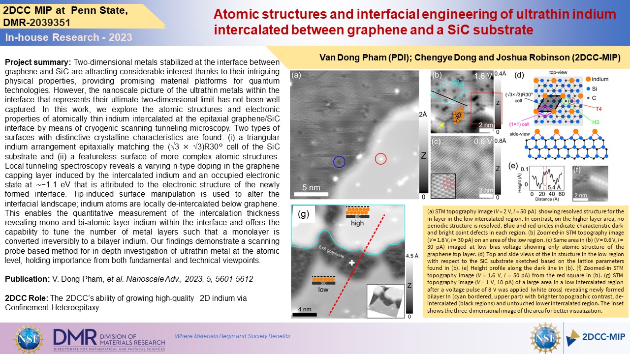
Project summary: Two-dimensional metals stabilized at the interface between graphene and SiC are attracting considerable interest thanks to their intriguing physical properties, providing promising material platforms for quantum technologies. However, the nanoscale picture of the ultrathin metals within the interface that represents their ultimate two-dimensional limit has not been well captured. In this work, we explore the atomic structures and electronic properties of atomically thin indium intercalated at the epitaxial graphene/SiC interface by means of cryogenic scanning tunneling microscopy. Two types of surfaces with distinctive crystalline characteristics are found: (i) a triangular indium arrangement epitaxially matching the (√3 × √3)R30° cell of the SiC substrate and (ii) a featureless surface of more complex atomic structures. Local tunneling spectroscopy reveals a varying n-type doping in the graphene capping layer induced by the intercalated indium and an occupied electronic state at ∼−1.1 eV that is attributed to the electronic structure of the newly formed interface. Tip-induced surface manipulation is used to alter the interfacial landscape; indium atoms are locally de-intercalated below graphene. This enables the quantitative measurement of the intercalation thickness revealing mono and bi-atomic layer indium within the interface and offers the capability to tune the number of metal layers such that a monolayer is converted irreversibly to a bilayer indium. Our findings demonstrate a scanning probe-based method for in-depth investigation of ultrathin metal at the atomic level, holding importance from both fundamental and technical viewpoints.
Publication: V. Dong Pham, et al. Nanoscale Adv., 2023, 5, 5601-5612
2DCC Role: The 2DCC’s ability of growing high-quality 2D indium via Confinement Heteroepitaxy
What Has Been Achieved: This work revealed the atomic structure of 2D indium between EG and SiC and established the ability to either de-intercalate or reconstruct the intercalated materials while the graphene top layer remains unaltered via tip-induced manipulation.
Importance of Achievement: In this work, we reveal the atomic and electronic structures, the intercalation thickness and the interfacial engineering of the 2D indium. Two atomic phases corresponding to monoatomic and bilayer In structures stabilized under graphene are revealed. On the In monolayer, a triangular lattice matching epitaxially with the (√3 × √3)R30° periodicity of the underlying SiC substrate is identified. In contrast, no clear indication of the atomic arrangement is probed for the In bilayer. This observation clearly demonstrates the significant importance of the SiC substrate as an epitaxial template for 2D crystalline In to be formed. We have successfully used tip-induced manipulation as a versatile tool to either de-intercalate or reconstruct the intercalated materials while the graphene top layer remains unaltered. This allows microscopic insight into the ultrathin In at the EG/SiC interface with respect to intercalation thickness, good control over the number of metal layers and thermodynamic stability of In at the interface.
Unique Features of the MIP That Enabled Project: Synthesis of high-quality 2D indium via confinement heteroepitaxy enables exploring atomic structure of one- or two-layer indium at EG and SiC interface.
Publication: Pham, van Dong, Dong, Chengye, and Joshua A. Robinson. "Atomic structures and interfacial engineering of ultrathin indium intercalated between graphene and a SiC substrate." Nanoscale Advances (2023).
Acknowledgments: This work is primarily supported by the National Science Foundation through the Penn State 2D Crystal Consortium - Materials Innovation Platform (2DCC-MIP) under NSF Cooperative Agreement No. DMR-2039351.