Semiconductors designed to deliver extreme capabilities

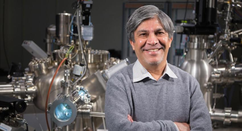
Student examines sample in Chu's lab

By Jamie Oberdick

Your cellphone probably would not work very well in space. That is because outer space is full of radiation, and radiation causes defects in electronics that can eventually lead to device failure. You and your cellphone are likely not going to be in outer space anytime soon, but if you are an astronaut relying on electronics to get you to and from space without incident, Rongming Chu’s research may one day be key in keeping you safe.

Packaging is a huge part of the semiconductor puzzle, and Penn State has answers

chip packaging

The big news around semiconductors, the factor that drove the CHIPS for America Act, was and is the supply chain. Many in the media focused on the shortages and disruption in the chips supply chain that was caused by the pandemic, and in turn, created big increases in the price of things like automobiles. But there is also another big deal happening with semiconductors that does not get as much attention – packaging.

Growing tomorrow’s semiconductor chips in the materials garden

terrones holds a sampl

In some ways, Mauricio Terrones is a gardener. An Evan Pugh University Professor and The Penn State Verne M. Willaman Professor of Physics, Terrones does not grow flowers or vegetables, but instead, one- or few-atom-thick two-dimensional (2D) materials. Specifically, creating materials with specific properties. The first 2D material ever created was graphene, and Terrones was a pioneer in developing 2D materials beyond graphene such as molybdenum disulfide (MoS2) and Tungsten disulfide (WS2). These are layered 2D materials, monolayered, bi-layered, tri-layered or more.