Q&A: How can advanced chip packaging help redesign the future of semiconductors?

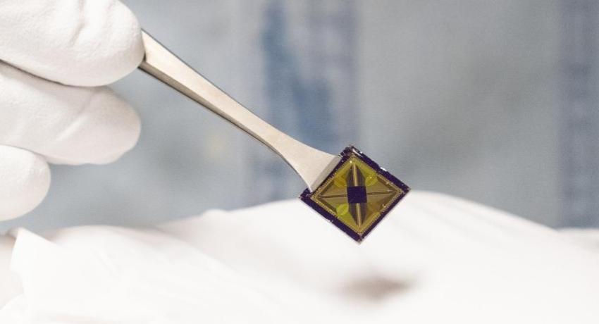
Microchips Image

Researchers explain how chip architecture and Penn State-led initiatives can help jump-start U.S. chip manufacturing

By Tim Schley

The phrase “advanced chip packaging” might conjure images of a fancy Pringles can. For those who manufacture semiconductors — also known as integrated circuits, chips or microchips — it represents a new frontier, a race to design and mass produce the next generation of semiconductors that use less energy while delivering more computing power.

‘Surprising’ hidden activity of semiconductor material spotted by researchers

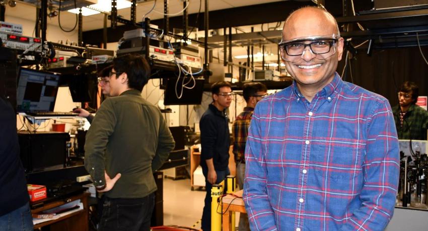
Prof. Gopalan in lab with students

By Jamie Oberdick

New research suggests that materials commonly overlooked in computer chip design actually play an important role in information processing, a discovery which could lead to faster and more efficient electronics. Using advanced imaging techniques, an international team led by Penn State researchers found that the material that a semiconductor chip device is built on, called the substrate, responds to changes in electricity much like the semiconductor on top of it.

Silicon Carbide Innovation Alliance to drive industrial-scale semiconductor work

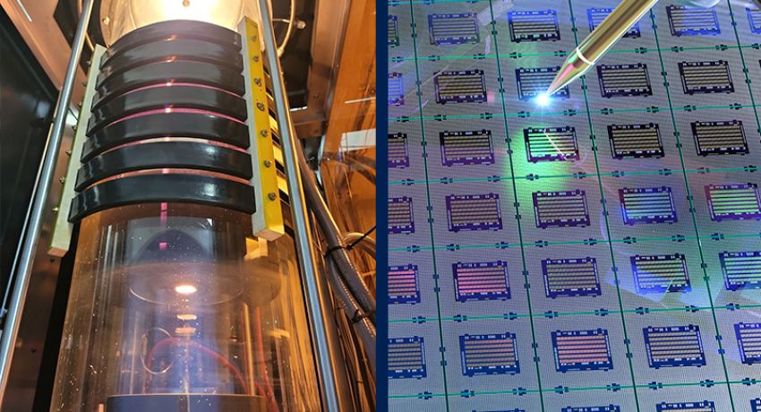
SCIA News Graphic

By Jamie Oberdick

Known for its ability to withstand extreme environments and high voltages, silicon carbide (SiC) is a semiconducting material made up of silicon and carbon atoms arranged into crystals that is increasingly becoming essential to modern technologies like electric vehicles, renewable energy systems, telecommunications infrastructure and microelectronics.  

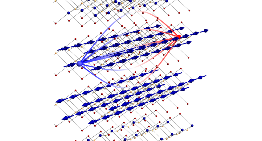
Can AI crave a favorite food?

AI Sensor for Taste Image

By Jamie Oberdick

'Electronic tongue' holds promise as possible first step to artificial emotional intelligence

Can artificial intelligence (AI) get hungry? Develop a taste for certain foods? Not yet, but a team of Penn State researchers is developing a novel electronic tongue that mimics how taste influences what we eat based on both needs and wants, providing a possible blueprint for AI that processes information more like a human being.  

Solution found to problem bedeviling semiconductor researchers

Sapphire substrates

By Jamie Oberdick

Researchers from the National Science Foundation-sponsored Two-Dimensional Crystal Consortium (2DCC-MIP) - Materials Innovation Platform may have come up with a solution for a bottleneck that has confounded researchers trying to develop high-quality 2D semiconductors for next generation electronics such as Internet of Things (IoT) and artificial intelligence.